PCB – what is the key component in electronics manufacturing?

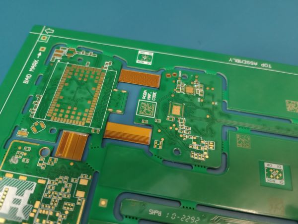
Today, printed circuits are with us at every turn. They are present in smart phones, computers, household appliances, as well as medical devices and aircraft. In an era of miniaturisation of electronics and increasing complexity of board designs both, PCB suppliers and PCB assembly factories, are meeting customer needs with innovative technical solutions and materials. What is the process of ordering a PCB and assembling the PCBA components? What are the challenges involved? The answers to these questions are provided by the work of Comarch IoT Plant, a state-of-the-art manufacturing facility offering services in the field of rapid prototyping and assembly of electronic devices (EMS).
What is a PCB?
PCB (Printed Circuit Board) is a printed circuit board with conductive paths (also called tracks) and soldering points, which come in two forms. The first form of points are pads used for surface mounting, the second are holes used for through-hole mounting. It is on the PCB that the electronics are then assembled. Then PCBA, i.e. Printed Circuit Board + Assembly, is what we are talking about.
– Printed circuits became popular in the second half of the 20th century. They were first used in radio receivers. Earlier, electronic connections were made using wires. However, this type of solution was laborious to install and, due to the large number of wires, cumbersome in terms of size. The advent of multilayer PCBs has finally made it possible to create compact devices with enhanced functionality – explains Mateusz Rosek, Quality Control Engineer at Comarch IoT Plant.
Building a PCB step by step
What are the key parameters and features of PCBs that the designer must include in the production design?
Laminate types – depending on the purpose of the circuit, we use different types of laminates and materials. They can be classified both in terms of popularity and interesting design application.
- FR-4 laminate – general-purpose laminate; from simple electronics to medical and military devices that do not impose requirements for high frequencies or high circuit thermal capacitance. This type is characterised by a glass transition temperature – Tg 140°C. Better frequency properties than FR4 are presented by Isola's FR408 laminate, which is used in RF circuits.
- RIGID FLEX laminate – a relatively new type of laminate among those available on the market. Its design differs from the standard one. Inside, instead of the FR4 laminate core that is most common, there is a polyamide-cored flexible section over which resin-coated copper foil is applied. The base thus built is then encased in FR-4 rigid laminate. The position of the FLEX layer can be asymmetrical – the number of copper layers on either side of the flexible core need not be the same. This solution streamlines designs where several boards are connected by connectors. FLEX laminates are characterised by flexibility – they allow flexible parts to be bent repeatedly without risk of damage.
- SEMI-FLEX laminates – unlike RIGID-FLEX, there is no polyamide core involved. A specially prepared part of the FR-4 laminate covered with a flexible soldermask is bent. In this case, the number of bending cycles is severely limited. This type of laminate is designed for one-off shaping of a flexible part during assembly, such as in an enclosure. Subsequent bending of the laminate can result in damage.
- PTEF laminate – specialised RF laminates made from ceramic or Teflon. They are designed for the manufacture of microwave circuits. They exhibit the best frequency properties and the highest glass transition temperature.
- Aluminium and copper laminate – these are special laminates used where high-power components, such as transistors that generate large amounts of heat, are mounted in an electronic circuit. In such a laminate, the core is made of an insulated aluminium or copper plate.
- HDI laminate – not distinguished from others by the use of an unconventional material – usually FR-4 laminates with better thermal and frequency properties or Isola or Rogers laminates. However, they feature a higher Tg than standard FR-4 laminates, reaching 185°C, and are therefore recommended for multilayer PCB designs. They are worth attention where there is a very dense occupancy of components on the laminate surface.
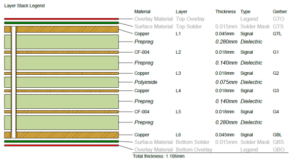
PCB layers – a PCB is built like a cake or a sandwich. The central part is the core. It is covered on one (single-layer) or both sides with alternating layers of copper foil etched with a mosaic of tracks and prepreg – a composite fibre impregnated with resin. During PCB production, the layer stack thus prepared is bonded in a press under high pressure and high temperature. Depending on the complexity of the project, the following board types are distinguished:
- 1-layer – the copper layer with tracks and pads only on one side of the laminate;
- 2-layer – the copper layer with tracks and pads on both sides of the laminate;
- multilayer – where component packing on the board is very dense, there is simply not enough room to route all the tracks over one or two layers. This solution is particularly popular when large BGAs are used. Depending on the number and type of circuits used, the number of layers can be 4, 6 or 8, but there are projects where 16 or even 20 layers of copper are required.
The purpose of the device requires the specific layer thickness. For example, in the power supply circuits, where high currents are involved, the copper layers will be thicker than in standard signal paths. The thickness of the copper layer is expressed in ounces (Oz) or micrometres (µm). As a standard (during PCB pressing, the thickness of both copper foil and prepregs may decrease slightly), the final thickness of the copper outer layer including finish is 35 µm (1 Oz), the same is assumed for the inner layers. If the project so requires, the thickness of both, the outer and inner layers can be increased to 70 µm, for example, and in extreme cases to 105 µm or 210 µm. It is also possible to reduce the thickness of the copper to 0.25 Oz.
– The number and thickness of the layers is also related to the width of the paths and the distances between the paths and the laminate layers. These criteria are critical to maintain specific path impedances. This is important in terms of eliminating the interference that can occur in the circuit and adversely affect the performance of the electronics assembled on the laminate – comments Mateusz Rosek.
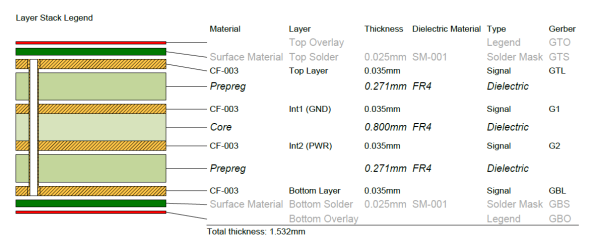
Vias – to connect two or more layers, it is necessary to use vias between individual layers. Vias are holes whose walls are metallised, thus providing an electrical connection between the specific layers. Standard vias are drilled, while micro vias – due to technical limitations – are made using a laser. There are 7 types of vias (Type I to Type VII), differing in the way they are covered or filled. Note that the via coverage can be single or double-sided. Due to the way the layers are connected, they can be divided into several main types:
- Through-hole vias – connect the outer layers of copper together.
- Blind vias – connect selected layers together. It can be a connection between the outer layer and the inner layer or between specific inner layers.
- Buried vias – connecting the inner layers together. Unlike blind vias, making this type of vias requires drilling into specific layers of the laminate.Microvias – vias with very small diameters only possible with a laser. Blind and buried microvias may also be present.
- Vias In Pad – made in pads, most commonly used to connect signals running from BGAs.
Pads and holes – at this stage, the PCB designer creates the outer layers of copper (or one outer layer in single-layer boards) with the following parts: pads, i.e. soldering points for surface mounting of components, and holes – for through-hole mounting or intended for positioning and mechanical mounting in a housing or target mounting location, such as on another PCB.
At this stage, it is very important to select the size and shape of the pads to match the components used in the project. For a surface assembly, this has a very strong impact on the correctness of soldering of components. Making a PCB footprint (pinout of an electronic component) that does not match the real footprint of the component can result in incorrect soldering of the component, e.g. the formation of so-called passive component tombstoning. This may also prevent the component from being soldered to the PCB. This will also be the case when the pads are made too small. Insufficient spacing between pads on SOPs, SOTs, QFNs or QFPs circuits can result in short circuits between the circuit pinouts.
The holes can be divided to:
- Plating Through Hole (PTH) – holes with metallisation passing through the board to form an electrical connection between layers. They are used for the assembly of through-hole components, e.g. electrolytic capacitors, relays, coils, as well as various types of connectors. In the case of the latter, it is worth mentioning press-fit connectors, in which the pins are not soldered, but pressed into metallised holes. In this case, the accuracy of such holes is critical to ensure that the connectors are permanently and correctly installed.
- Non Plating Through Hole (NPTH) – holes without metallisation passing through, not forming an electrical connection. Usually used for positioning components on a PCB or assembling the board itself in a housing or other destination.
The holes can be of different shapes and sizes depending on the application. As with the pads, it is critical to maintain an adequate footprint in the design to allow the components to be installed correctly.
Board thickness – using a large number of PCB layers, as well as thicker copper layers, will increase the thickness of the finished laminate. The standard plate thickness is 1.6 mm. The thickness of more complex boards is 2 mm, but PCB suppliers already offer laminates as thick as 6 mm. However, there are occasions when a PCB has to be mounted in a place or in a housing where a standard 1.6 mm thick board will not fit. In such cases, the designer can create a board that is 1.1 mm, 0.6 mm or even thinner. The thinnest PCB I have had my hands on in my IoT Plant career was 0.6 mm thick.
Soldermask – is a protective mask that protects the surface of the PCB against both corrosion and uncontrolled solder flow. The soldermask covers the entire PCB surface except for pads and PTH holes, as well as vias if the specification requires so. The soldermask is applied as a liquid paint cured by UV light. On this occasion, it is worth mentioning the peelable mask, applied by screen-printing. This is a so-called temporary mask, protecting, for example, solder holes from being filled with alloy during the SMT or THT process. Once the soldering is finished, such a mask can be detached to proceed to the next assembly steps. The soldermask comes in a variety of colours, but the standard is (the cheapest) green. On request, the factory can use a different colour, e.g. black, blue, red.
Finish – a.k.a. plating, describes the material that protects the pads from corrosion, as well as other areas of copper not covered by the soldermask. The types of plating differ in price, durability as well as environmental impact. Among these we can mention:
- HASL (Hot Air Solder Leveling) – the simplest and the cheapest way to finish a PCB. It involves coating exposed copper parts with a tin-lead solder alloy. By default, this is a lead-containing alloy, but also the HASL Lead Free, which, as the name suggests, is a lead-free alloy, can be used if necessary. The main advantage of this finish is the low cost. The drawbacks include variations in finish thickness depending on pad size, which can cause difficulties in soldering small components or short circuits between circuit leads.
- Immersion Tin – chemical tinning ensures a flat pad surface and good solderability. The main flaw here is the susceptibility to dirt and contamination, which can hamper the soldering process and a process that leaves behind substances that are harmful to the environment.
- ENIG (Electroless Nickel/Immersion Gold) – a chemical method of coating copper with a base layer of nickel followed by a layer of gold. This method also provides a flat pad surface, excellent solderability and extended storage time for electronic circuits. The disadvantage is the high cost of production.
- OSP (Organic Solderability Preservatives) – an organic finish coating to ensure a flat pad surface and good solderability. The disadvantages are a short shelf life and rapid degradation in the multi-pass soldering process.
- Gold Fingers – a specific type of chemical gold plating used for edge connectors, e.g. expansion card connectors in computers. This type offers high mechanical strength, i.e. resistance to abrasion. Gold Fingers are usually applied to the connector, while a different type of plating, such as ENIG, is applied to the rest of the PCB.
Silkscreen – an ink layer applied to the soldermask, also known as a legend or descriptive layer. It usually comes in white. If the colour of the soldermask is light, black silkscreen is used for better contrast and legibility. The information provided in the description layer includes component designators and outlines, polarity markings, connector designations or the manufacturer's logo. Provision of the legend is not obligatory in PCB production, and is entirely up to the customer.
Panelization – by default, the PCBs are designed as a single board. However, in order to maximise the use of laminate material and optimise surface or through-hole assembly, individual PCBs are arranged in an array. Two main methods of panelization can be distinguished – grooving (cutting on both sides of the board) and milling (machining the shape of the board into the panel).
Fiducials – these are technical markers that serve as reference points for machines on the PCB surface. Fiducials can come in a variety of shapes (circles, circles, squares, crosses, triangles) and are typically 1-1.5mm in size. Fiducials are recommended to be placed on the panel envelope as well as on each perimeter separately. Fiducials should be located on both sides of the PCB. They should also be away from the edges of the panel/PCB and from testpoints or holes of similar size that could be identified by machines as fiducials. Typically, fiducials are placed in the three corners of the panel.
What files are needed in Comarch IoT Plant to place a PCB order?
– The basic files required to order PCBs in Comarch IoT Plant are the Gerber files. They define all the layers of copper foil, their shape, paths, pads, the milling or chiselling a path that defines the shape of the PCB and the soldermask layers, as well as the screen-printing layers – says Mateusz Rosek.
Also directly linked to Gerber files are the drill files containing information on vias and holes. These files can be provided separately as files of each layer and drillings for PTH and NPTH holes or as one package in ODB++ or tgz format.
Another indispensable piece of documentation needed to order a PCB is a specification determining the number and thickness of layers, the dimensions of the board, the type of material and finish, and the method of depaneling. For multilayer circuits, it is helpful to expand the specification to include a so-called stack-up, which is a graphical or textual representation of the board cross-section including the thickness of the core, copper layers and prepregs. The specification may also include details on the target impedance values of specific paths in multilayer circuits.
If the customer does not specify panelization in Gerbers files, at Comarch IoT Plant, we come up with our own panel proposal ensuring optimal PCB alignment, which in turn ensure efficient and correct assembly of electronic components. Once the customer approves the panel proposal, it is included in the PCB order. If panelization is provided in the form of bridges, the milling layer contained in the Gerber files is required for the depaneling process.
What do we look for when reviewing a PCB design?
To ensure the efficiency of the Comarch IoT Plant processes, the documentation provided by the customer is always subject to review by our engineers. For the customer-panelized PCB, we check that the panel can be handled by our machines. Due to technical constraints, we aim for a panel size of no more than 350 × 300 mm. Sometimes we suggest to the customer that the panel layout be changed to improve stiffness. This mainly applies to wide panels where there are many small tiles. Another thing we look out for are the various types of connectors that are installed close to the edge of the PCB or that extend beyond the outline of the board. Here, three factors come into play:
- The use of grooving panelization while placing connectors directly at the edge or protruding beyond the PCB outline to prevent depaneling.
- Bridges (breakaway tabs) that are too close to the connector or directly underneath the connector that may make depaneling difficult or impossible. If necessary, we recommend repositioning the bridges or changing the type of panelization.
- Connectors with positioning tabs on the underside of the housing, which require appropriate cut-outs in the PCB laminate or panel envelope.
In the next step, we check the position of the fiducials – critical for all the processes carried out automatically on the machines. This is because if the machine does not find a reference point, it will not be able to perform the programmed actions. For this reason, one of our requirements is to place the fiducials on both sides of the panel, a minimum of 4 mm from the outer edge of the panel.
Once we have received all the comments, we consult with the customer to arrive at the optimum form of PCB panel.
Comarch IoT Plant collaboration with proven and reliable PCB suppliers
Since entering the market, we have succeeded in establishing partnerships with a number of PCB suppliers offering services on the global and European markets. To date, the Comarch IoT Plant team has worked with a network of top-quality suppliers on medical, military and space equipment projects. These are companies that specialise in challenging multi-layer tile projects, have access to a wide range of materials for specialist applications and meet specific, exacting standards.
– From the moment you send us your enquiry, we have the full support of the supplier's representatives. Valuable feedback from the factory is often available at this stage, with specific suggestions for improvement. We then go through a phase of technical questions, where all the details of the PCB production are agreed – adds Mateusz Rosek.
Key process elements: storage, PCB defects and PCB input inspection
After production at the factory, the PCBs are packed hermetically in vacuum bags, fitted with moisture absorbers and moisture indicators. The former absorb the moisture sealed in the bags during sealing, while the latter make it possible to determine whether the packaging has become unsealed during transport.
– Moisture is the number one enemy of printed circuit boards. Firstly, with some PCB finishes, it promotes corrosion on the surface of the pads. Secondly, it can cause much worse damage to the board. If moisture penetrates the structure of the board, it can lead to swelling and delamination of the laminate – comments Mateusz Rosek.
Such a defect may not be immediately visible, sometimes it only becomes apparent at the soldering stage, when in the furnace, under the influence of high temperatures, water particles trapped in the PCB structure begin to boil, causing the laminate to burst. Such defects can also occur at the laminate production stage if the material has been stored incorrectly, allowing the fibre sheets to absorb moisture.
Failures in the production of PCBs can occur even in the absence of moisture, as a result of incorrectly chosen process parameters, which can lead to the laminate being improperly compressed and result in the delamination. Such defects are usually detected by quality control at the PCB factory, but at Comarch IoT Plant we check the boards for design compliance and mechanical damage once they are delivered to us.
Comarch IoT Plant – PCBA assembly and much more
– We perform PCBA assembly services at Comarch IoT Plant, a state-of-the-art manufacturing facility located in the heart of Krakow. We consider PCBs to be one of the key components in electronics manufacturing, so we take great care to order them from verified sources, from trusted suppliers. They also undergo a series of control processes to ensure the ultimate success of the project – says Mateusz Rosek.
Our customers can rely on our support at every stage of electronics development – from the idea and prototype to production and testing of the device. The IoT Plant's services include surface mount (SMT) and through-hole (THT) assembly, including simple or selective wave soldering and hand soldering. We also offer recovery and repair of electronics. As part of our quality testing, we subject it to a wide range of tests: automatic optical inspection (AOI) and X-RAY (AXI) iCT (In Circuit Test), FCT (Functional Tests), ICSP (In-Circuit Serial Programming), Flying Probe and environmental tests.
To find out more about what benefits your company can gain from working with our plant floor, visit the Comarch IoT Plant website.